What is
Porous Silicon?
Porous Silicon is one of the most exciting materials being tested and characterized throughout the research world. Future technological breakthroughs in electronics, e-mobility, consumer goods, solar, sensors, and medicine, to name a few, are happening now largely through the use of porous silicon.
Because of its abundance, electrical properties, and bio-compatibility silicon has been and will continue to be an important material for many high tech industries. By taking advantage of the material properties as well as the geometrical and volumetric properties after etching pores into silicon substrates and particles, new and exciting applications are bringing these breakthroughs with in reach
In the 1950's,
two engineers at Bell Labs were trying to develop a process for shaping and polishing Silicon and Germanium wafers. After various attempts of mixing HF acid and solvents with applied current on the Silicon surface, not much was thought to have happened other than a change in surface color from a blackish to reddish brown.
These results ...
Since this (re)discovery of the quantum confinement properties, porous Silicon has become interesting not only for photoluminescence, but for solar applications by trapping more light or photons within the Si cell, more electricity can be produced. The beauty of the porous Silicon process is that depending on the mix of chemistry and levels of applied current, the pores or porous surface can be finely tuned altering the refractive index, volume density, surface area and overall porosity from a bulk Silicon wafer to a Silicon sponge layer or all the way to a Silicon cloud or web.
Later these highly porous structures have been used as a scaffolding for thin film deposition, membranes, epitaxial layers for sensors, wearable electronics and even for growing and grafting human skin.
In the 1990's,
Types of Porous Silicon
Porous Silicon is generally separated into 3 different categories according to the pore diameter.
1. Microporous
pore size <5nm
2. Mesoporous
pore size 5nm – 50nm
3. Macroporous
pore size >50nm

FAQ

Theoretically Silicon is Silicon so yes batteries can be made from high purity porous Silicon which is also safe for the human body. However, the cost for high purity and finely tuned electro-chemically etched Silicon for medical application isn’t pragmatic for a cost effective battery anode.
By buying mined or metallurgic bulk Si in kg and/or in tons instead of wafers the intial material costs can be driven way down. This comes, however, at the expense of jeopardizing the purity levels which are then no longer acceptable or safe within the body.
The price can also be reduced further by etching without electricity. A so called chemical etch or stain etch is a much simplified process that results in wider pore diameter ranges and overall lower porosities. This works well for batteries, but becomes difficult to consistantly load for medicinal purposes.
Silicon, Hydrofluoric acid, solvent, current density.
By applying a voltage across the top and bottom of a Silicon Wafer, charge carriers for instance (positive holes in p-type Si) within the Si migrate to the HF/Si Interface. HF alone etches away any oxide found on the surface creating a hydrophobic Si surface.
The solvent in the HF mixture helps to create a stabile contact between the HF and Si especially as etching takes place deep underneath the orginal surface. As Si, HF and +holes come together, the Si is carried off creating H2 gas and leaving a pore. The pore size is controlled by current density, HF concentration, and Si resistivity(Charge carriers).
Photo-etching is a process used to fabricate precision metal parts. It is also called Photo Chemical Machining (PCM) and is an alternative to metal stamping, laser cutting, water-jet cutting, and electric discharge machining (EDM). Metal parts or sheets that are produced by photo-etching processes are more accurate and economical as compared to other machining methods.
Like any other printing process, photo-etching duplicates part dimensions on a photo-resist coated metal. It was developed soon after the materialization of the printed circuit board (PCB) industry and has become widely popular since then. It works best with metals of thickens from 0.0005 to 0.080 inches, or 0.013 to 2.032 mm.
Applications of photo-etching include several commercial metals or alloys such as steel, stainless steel, aluminum, brass, nickel, titanium, and silver. Ideally, it is used for the production of fine screens and meshes, metal seals, heat sinks, sensors, circuit components, flexible heating elements, EMI/RFI shields, jewelry, and in many other manufacturing industries.
Several metals are eligible for photo-etching thus allowing a large array of options to choose the metal according to requirements of the customer. To begin the process, once the metal type is finalized; the desired customer design is printed onto a photographic film. This is called a photo-tool. It is dimensionally stable and has two sheets. The image is shown in these sheets in its negative form, black and clear areas. The black portions represent the parts to be etched.
The photochemical machining process contains a series of steps. First of all, raw metal sheets are cut according to the required size. Before proceeding any further, they are properly cleaned using chemicals to remove excess particles, debris, oils, or waxes. After that, it is coated and both sides are laminated with an ultraviolet sensitive photoresist. This photoresist enhances accuracy and improves the quality of the material. Coating of the product is carried out via an automated process. After cutting, cleaning, and coating, the material is headed for printing.
The coated material sheets are kept between the two photo-tool sheets for the printing process. The space between metal sheets and photo-tool is optimized by vacuum. Then it is passed through ultraviolet light. The UV light application hardens the exposed area and the non-exposed parts remain soft. The unexposed soft resist can be washed away from the printed sheets. The hard exposed resist does not come off during this wash and the underlying material also remains intact during etching.
Following this, metal sheets are ready for etching. In this process, the metal sheets are exposed to a pressurized and heated acidic solution. Ferric chloride is commonly used for this purpose. The chemical solution reacts quickly with the unprotected metal surfaces and corrodes them efficiently. In this way, parts from the original photographic film are retained. Metal sheets are then neutralized and rinsed thoroughly to remove the remains of photoresist. Subsequently, the photo-etched parts are cleaned, dried, and subjected to visual and dimensional inspection. Post-etching, finishing steps are performed for enhancement like polishing, bonding, and coating as per the final application.
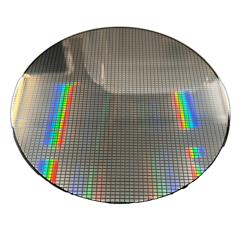
Micro, Meso-, Macro- wafers, films and particles
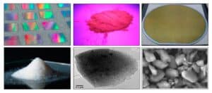
Pore diameters from 1nm to 1μm.
Wafers sizes 4,6, and 8 inch.